- Overview
- Ceramic pcb Capability.
- Applications of Ceramic PCB
- Types of Ceramic PCB
- Company Profile
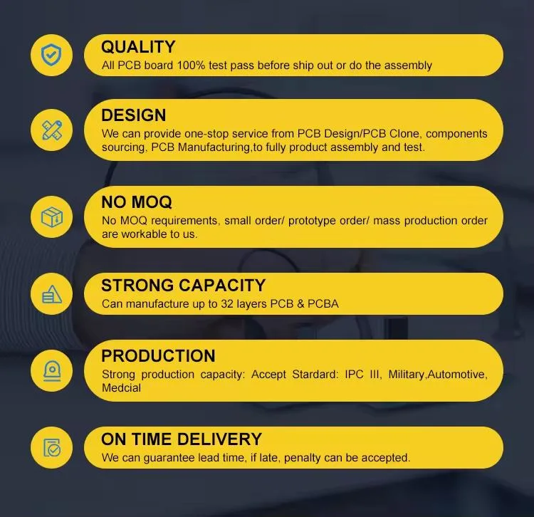
- Our Advantages
- Product Description
- Certifications
- FAQ
Basic Info.
Product Description

| Board Thickness(mm) | 0.25/0.38/0.5/0.635/1.0/1.5/2.0/2.5/3.0mm |
| Layer Number | 1-2L |
| Base copper thickness(um) | 18-300um(0.5-8.5oz) |
| Min Track width/space(mm) | 0.075mm |
| Min hole size | 0.06mm(PTH) |
| Finished hole tolerance(mm) | 0.05mm(NPTH) |
| Outline Tolerance(mm) | 0.05mm |
| Hole Tolerance | +/-0.05mm |
| Min space from track to board edge | 0.2mm |
| Finished board thickness | (0.25-0.38mm)+/-0.03mm |
| (0.38-0.635)+/-0.04mm | |
| (0.76-2mm)+/-0.05mm | |
| Surface Treatment | ENIG,ENEPIG,Immersion Silver |
| Material | ALN, AL203 |
As a Ceramic PCB Supplier in China, we can support our customers from prototype to mass production. we are not only focusing on single-layer boards but also Multilayer circuit boards.
| Color | / | White | 3.2 |
| Density | g/cm³ | ≥ 3.7 | GB/T 2413 |
| Thermal Conductivity | 20ºC, W/(m • K) | ≥ 24 | GB/T 5598 |
| Dielectric Constant | 1MHz | 9~10 | GB/T 5594.4 |
| Dielectric Strength | KV/mm | ≥ 17 | GB/T 5593 |
| Flexural Strength | Mpa | ≥ 350 | GB/T 5593 |
| Camber | Length‰ | ≤2‰ | |
| Surface Roughness Ra | µ m | 0.2~0.75 | GB/T 6062 |
| Water Absorption | % | 0 | GB/T 3299-1996 |
| Volume Resistivity | 20ºC, Ω .cm | ≥ 1014 | GB/T 5594.5 |
| Thermal Expansion | 10-6 mm 20~300ºC | 6.5~7.5 | GB/T 5593 |
Even though the ALN PCB will be more expensive than the AIO203, ALN has high conductivity, and the expansion coefficient matching Si, which makes the customers still choose it as the material for their products, here you can see the details for the ALN material properties.
| ITEM | UNIT | VALUE | TEST STANDARD |
| Color | / | Gray | 3.2 |
| Density | g/cm³ | ≥ 3.33 | GB/T 2413 |
| Thermal Conductivity | 20ºC, W/(m • K) | ≥ 170 | GB/T 5598 |
| Dielectric Constant | 1MHz | 8~10 | GB/T 5594.4 |
| Dielectric Strength | KV/mm | ≥ 17 | GB/T 5593 |
| Flexural Strength | Mpa | ≥ 450 | GB/T 5593 |
| Camber | Length‰ | ≤2‰ | |
| Surface Roughness Ra | µ m | 0.3~0.6 | GB/T 6062 |
| Water Absorption | % | 0 | GB/T 3299-1996 |
| Volume Resistivity | 20ºC, Ω .cm | ≥ 10¹³ | GB/T 5594.5 |
| Thermal Expansion | 10-6 mm 20~300ºC | 2~3 | GB/T 5593 |

LED field
High-power semiconductor modules,
Semiconductor coolers,
Electronic heaters,
Power control circuits,
Power hybrid circuits,
High-frequency switching power supplies,
Automotive electronics,
Communications,
Aerospace.
Ceramic PCB Design Rules:


Ceramic Printed Circuit Boards (PCBs) come in various types and configurations, each designed to cater to specific applications and performance requirements. Here are some common types of ceramic PCBs:
- Single-Layer Ceramic PCBs: These are basic ceramic PCBs with a single conductive layer on a ceramic substrate. They are often used for simple applications where high thermal conductivity is needed but complex circuitry is not required.
- Multilayer Ceramic PCBs: These PCBs consist of multiple layers of ceramic substrates, with conductive traces and vias connecting the different layers. Multilayer ceramic PCBs are suitable for complex circuit designs, high-density interconnects, and applications requiring signal integrity.
- Thick Film Ceramic PCBs: In this type, thick film technology is used to create conductive and resistive traces on ceramic substrates. Thick film ceramic PCBs are known for their durability, making them suitable for applications in harsh environments like automotive and industrial settings.
- Thin Film Ceramic PCBs: Thin film technology involves depositing thin layers of conductive and insulating materials onto the ceramic substrate. Thin film ceramic PCBs offer precise electrical properties and are commonly used in high-frequency applications, such as RF and microwave devices.
- Hybrid Ceramic PCBs: These PCBs combine ceramic materials with other materials, such as organic substrates or metal cores. The hybrid approach allows engineers to balance the benefits of ceramics with the advantages of other materials, such as cost-effectiveness or specific thermal properties.
- Alumina (Al2O3) Ceramic PCBs: Alumina ceramic PCBs are made from aluminum oxide and are known for their high thermal conductivity, electrical insulation, and mechanical strength. They are suitable for various applications, including power electronics, LED modules, and high-power RF devices.
- Aluminum Nitride (AlN) Ceramic PCBs: Aluminum nitride ceramic PCBs offer even higher thermal conductivity than alumina, making them suitable for applications where efficient heat dissipation is critical. They are often used in high-power electronic devices and LEDs.
- Beryllium Oxide (BeO) Ceramic PCBs: Beryllium oxide ceramic PCBs are characterized by extremely high thermal conductivity and are used in applications that demand efficient heat dissipation, such as high-power RF amplifiers.
- Silicon Carbide (SiC) Ceramic PCBs: Silicon carbide ceramic PCBs are known for their excellent thermal and electrical properties, as well as their ability to withstand high temperatures and harsh environments. They are used in high-temperature electronics and power electronics.
- LTCC (Low-Temperature Co-fired Ceramic) PCBs: LTCC technology involves co-firing multiple layers of ceramic substrates at relatively low temperatures. LTCC ceramic PCBs are used in RF modules, sensors, and other miniaturized devices.


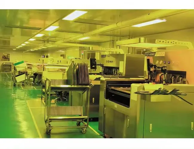
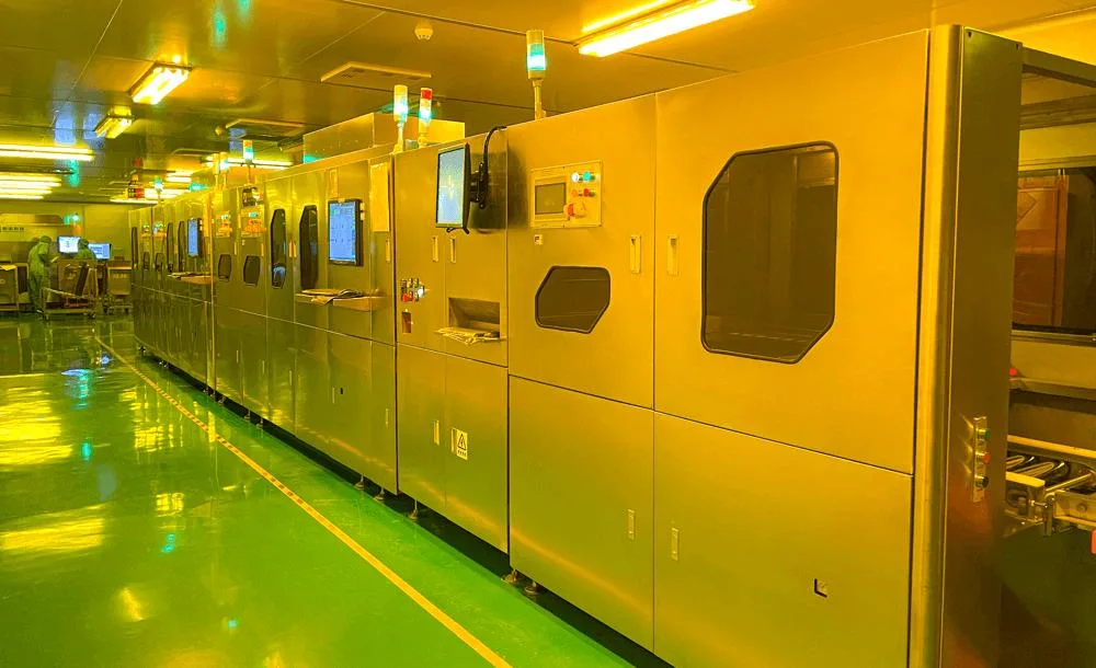
Shenzhen Jinxiong Electronics Co., Ltd as one-turnkey PCB and assembly provider, we specialize in PCB fabrication, PCB assembly and components sourcing services.
Professional PCB electronics manufacture services , such as Multi-layer PCB,HDI PCB,MC PCB, ,Rigid Flex PCB,Flex PCB.We can fabricate Laser holes ,Impedance Control PCB, Buried & Blind Holes PCB, Countersunk hole , other special material or special process PCBs.
About testing,we provide SPI Inspection, AOI Inspection, X-ray Inspection, ICT Testing and Functional Testing as our value-added services.
Stencil manufacturing techniques include chemical etching, laser cutting and electroforming. we provide the Magnetic stencil, frame SMT stencils and Frameless SMT stencil .
Ceramic PCB VS Fr4 Material
- Better thermal expansion
- Stronger and lower resistance metal film
- Good solderability of the substrate and high operating temperature 5, Good insulation, and Low High-frequency loss
- High-density assembly possible
- It has a long life and high reliability in aerospace as it does not contain organic ingredients and is resistant to the cosmic rays

Ceramic Printed Circuit Boards (PCBs) offer several advantages that make them highly desirable for various applications, especially those demanding high performance, reliability, and efficiency. Here are some of the key advantages of ceramic PCBs:
- High Thermal Conductivity: Ceramic materials, such as alumina (Al2O3), aluminum nitride (AlN), and silicon carbide (SiC), have excellent thermal conductivity. This means ceramic PCBs can efficiently dissipate heat generated by components, preventing overheating and ensuring reliable operation of high-power electronics.
- Excellent Electrical Properties: Ceramic materials exhibit low dielectric loss and exceptional electrical properties, particularly at high frequencies. This makes ceramic PCBs well-suited for applications in radio frequency (RF), microwave, and high-speed digital circuits, where signal integrity and low signal loss are critical.
- Mechanical Strength and Durability: Ceramic PCBs possess greater mechanical strength and rigidity compared to organic PCBs. This robustness enables them to withstand mechanical stress, vibration, and shock, making them suitable for applications in challenging environments.
- Chemical Resistance: Ceramics are highly resistant to chemicals, solvents, acids, and bases. This resistance makes ceramic PCBs well-suited for applications in industries where exposure to harsh chemicals is common, such as automotive, aerospace, and industrial sectors.
- High-Temperature Tolerance: Ceramic PCBs can withstand higher temperatures compared to traditional organic PCBs. This capability is crucial in industries like automotive and aerospace, where electronics must operate reliably in elevated temperatures.
- Miniaturization: Ceramic PCBs can accommodate fine traces, smaller components, and high-density interconnects, allowing for the design of compact electronic devices. This feature is essential for applications requiring miniaturization without sacrificing performance.
- Signal Integrity: Ceramic PCBs offer superior signal integrity due to their low loss tangent and high dielectric constant, especially at high frequencies. This makes them suitable for high-speed data transmission and communication systems.
- Harsh Environment Compatibility: Due to their thermal, mechanical, and chemical resistance properties, ceramic PCBs are well-suited for applications in harsh environments, such as oil and gas exploration, aerospace.
- Reliability and Longevity: The combination of high thermal performance, robustness, and chemical resistance contributes to the long-term reliability of ceramic PCBs, reducing the risk of failure and improving the lifespan of electronic devices.
- Customization: Ceramic PCBs can be customized to meet specific design requirements, including substrate material, layer configuration, trace layout, and component placement. This flexibility allows engineers to optimize the board's performance for a given application.
- EMI/EMC Performance: Ceramic materials inherently provide better electromagnetic interference (EMI) and electromagnetic compatibility (EMC) performance due to their electrical properties and shielding capabilities.

The fabrication process of Ceramic Printed Circuit Boards (PCBs) involves several steps that transform ceramic substrates into functional electronic circuits. The process may vary depending on the specific type of ceramic PCB and the manufacturer's capabilities, but here is a general overview of the steps involved in the fabrication of ceramic PCBs:
1.Design and Layout:
The process begins with the design of the circuit layout using computer-aided design (CAD) software. Components, traces, vias, and other elements are placed and routed on the layout, considering factors such as thermal management and signal integrity.
2.Substrate Preparation:
Ceramic substrates are chosen based on the application's requirements, such as thermal conductivity and electrical properties. The ceramic substrate is prepared by cutting, shaping, and polishing to the desired dimensions and surface finish.
3.Layer Preparation (for Multilayer PCBs):
For multilayer ceramic PCBs, individual ceramic layers are prepared and fabricated. These layers will eventually be stacked and interconnected. Each layer may undergo processes such as screen printing, where conductive and insulating pastes are applied to create circuit traces and insulation layers.
4.Conductive Layer Deposition:
Conductor materials, often metal pastes containing silver or gold particles, are applied to the substrate using techniques like screen printing or inkjet printing. These conductive traces will carry electrical signals between components.
5.Via Drilling and Filling:
Vias, which are small holes that connect different layers of the PCB, are drilled using laser or mechanical drilling techniques. The vias are then filled with conductive or non-conductive materials to establish connections between layers.
6.Firing or Sintering:
The ceramic substrate with applied conductive materials is fired in a high-temperature furnace. This process sinters the ceramic and fuses the conductive materials, creating a solid and durable circuit structure.
7.Additional Layering (for Multilayer PCBs):
The process of applying conductive traces, insulating layers, and vias is repeated for each layer in the multilayer stack.
8.Component Attachment:
Components, such as surface-mounted devices (SMDs), are attached to the ceramic PCB using soldering or specialized adhesives. Due to the high thermal conductivity of ceramics, specific soldering techniques may be required to ensure proper bonding.
9.Testing and Inspection:
The assembled ceramic PCB is subjected to various tests, including continuity checks, electrical testing, and potentially environmental testing. Inspection processes help identify defects and ensure the PCB's functionality and reliability.
10.Finishing and Coating:
Protective coatings or encapsulants can be applied to safeguard the PCB from environmental factors such as moisture, chemicals, and temperature variations.
11.Final Testing:
The completed ceramic circuit board undergoes final functional testing to ensure it meets the specified requirements and operates correctly.
12.Packaging and Delivery:
Once the ceramic PCB passes all tests and inspections, it is packaged and prepared for delivery to the customer or further integration into electronic devices.


Q1.What files for quotation?
A:PCB files(gerber), BOM list, XY Data(pick-N-place).
Q2.MOQ and what is KXPCBA fastest delivery time?
A:MOQ is 1pcs. Sample to mass production all can be supported by KXPCBA.
Q3.For PCB quotation , what files format do KXPCBA need?
A:Gerber, Protel 99SE, DXP, PADS 9.5, AUTOCAD,CAM350 are OK.
Bare PCB prototype PCBA(PCB Assembly)
Layer Quick turn Quantity Quick turn
2layer: 24hours <30pcs 1 days
4layer: 48hours 30-100pcs 2 days
6-8layer: 72hours 100-1000pcs 5 days
Q4.How to test PCB and PCBA boards?
A:SPI, AOI,X-RAY, FOC for PCBA (PCB assembly)
AOl, Fly probe testing, Text fixture testing, FOC etc for bare pcb.
Q5.Can you do PCB or circuit design?
A:Yes, we have design team including software,
hardware and structure engineers. We can supply
customized design service, Give your idea we can make it true.
