Basic Info.
Model NO.
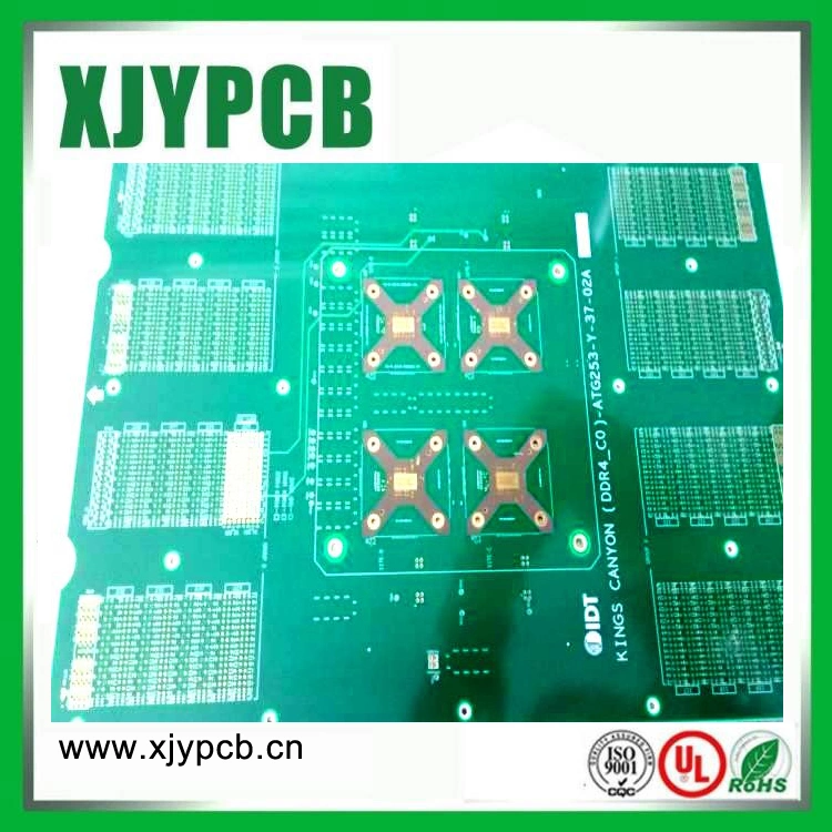
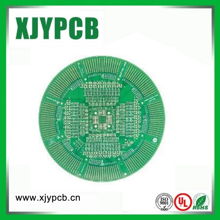
XJY-PCB 237
Production Process
Subtractive Process
Base Material
Fr4
Insulation Materials
Organic Resin
Copper Thickness
1oz
Surface Finishing
Immersion Gold
Solder Mask Type
Green
Silkscreen
White
Board Thickness
1.6mm
Min. Hole Size
0.15mm
Min. Line Width
0.1mm
Min. Line Spacing
0.1mm
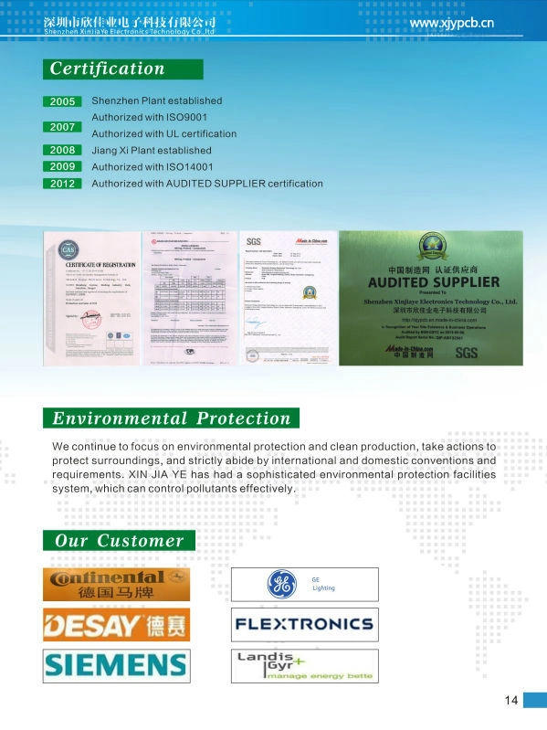
Certificates
UL, RoHS, SGS, ISO9001
Shipping
DHL, UPS, TNT, FedEx, etc
Transport Package
Vacuum Package
Specification
Normal
Trademark
OEM
Origin
China
HS Code
85340090
Production Capacity
20000 Square Meter/Square Meters / Month
Product Description
Welcome to XJY--------------
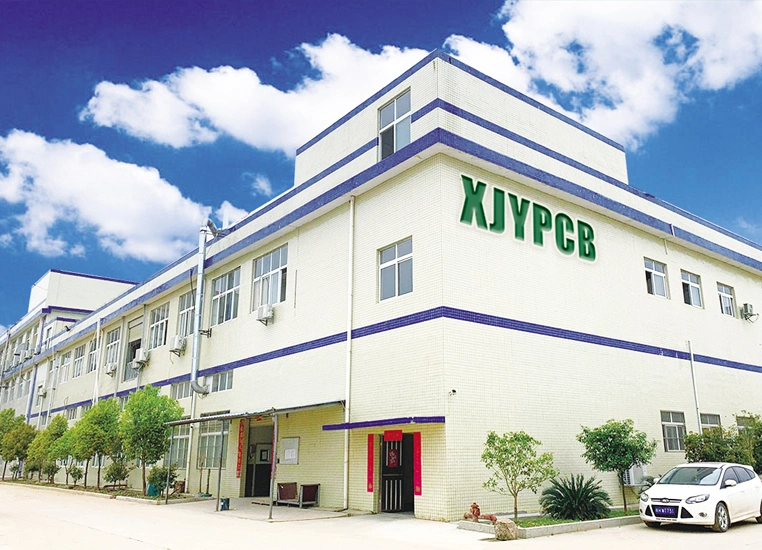
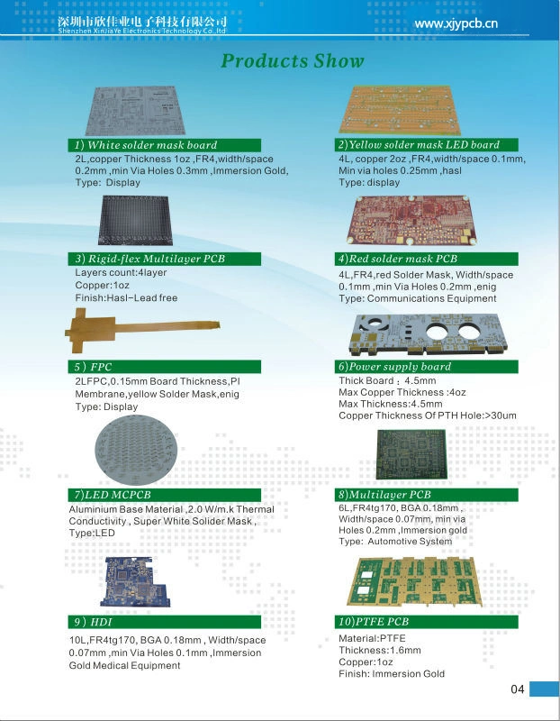
Shenzhen Xinjiaye Electronics Technology Co., Ltd is a professional pcb manufacturer has over 10 years experience. We are able to offer 1 to 24 Layer PCB, ranging from pcb produce, components purchase, pcb assembly, pcb copy service.Our products are widely used in communication apparatus, automobile electronics, auto parts, computers, medical devices, light systems, outdoor systems, network devices and consumer electronics class fields.
====+++++======
Quick Details
=====+++++=====
Technology capability
++++++Our PCB board manufacture and PCB assembly service++++++
1. PCB board file with parts list provided by customers
2. PCB board made, circuit board parts purchased by us
3. High Quality, competitive Price & Best Service
4.100% E-tested PCB
++++++Testing Procedures For PCB Board++++++
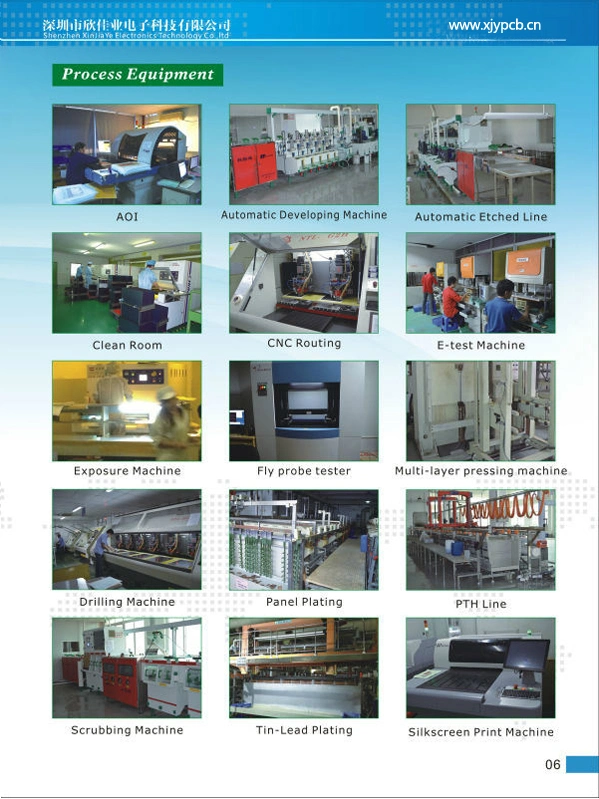
---We perform multiple quality assuring procedures before shipping out any PCB board. These include:
* Visual Inspection
* Flying probe
* Impedance control
* Solder-ability detection
* Digital metallograghic microscope
* AOI (Automated Optical Inspection)
++++++Following specifications are needed for quotation++++++
A) Base material
B) Board thickness
C) Copper thickness
D) Surface treatment
E) color of solder mask and silkscreen
F) Quantity
++++++Delivery Time for PCB board++++++
1) PCB production time: Sample: 3-4 days / mass production: Within 7 days
2) Component purchase: 2 days if all components is available in our domestic market.
3) PCB Assembly: Samples: Whthin 2 days / mass production: Within 5 days
++++++Shipping Method and Payment terms++++++
1. By DHL, UPS, FedEx, TNT using clients account.
2. We suggest you using our DHL, UPS, FedEx, TNT forwarder.
3. By EMS (Usually for Russia Clients), price is high.
4. By sea for mass quantity according to customer's requirement.
5. By customer's Forwarder
6. By Paypal, T/T, West Union, etc.
We sincerely hope to establish longtime and friendly business relationship with you. If you have interest in our product, please don't hesitate to contact us!


Shenzhen Xinjiaye Electronics Technology Co., Ltd is a professional pcb manufacturer has over 10 years experience. We are able to offer 1 to 24 Layer PCB, ranging from pcb produce, components purchase, pcb assembly, pcb copy service.Our products are widely used in communication apparatus, automobile electronics, auto parts, computers, medical devices, light systems, outdoor systems, network devices and consumer electronics class fields.
====+++++======
Quick Details
Place of Origin: | Guangdong, China (Mainland) | Brand Name: | XJY-PCB | Model Number: | xjypcb 237 |
Base Material: | FR4 | Copper Thickness: | 1oz or customized | Board Thickness: | 0.2mm-6.0mm |
Min. Hole Size: | 0.15mm | Min. Line Width: | 0.1mm | Min. Line Spacing: | 0.1mm |
Surface Finishing: | HASL or ENIG | solder mask color: | white ,Green,or customized | legend color: | White or customized |
copper thickness: | 1oz or customized | board thickness: | 1.6mm or customized | surface treatment: | variable according to your product |
substrate: | FR4 or Al or other | Layer Counts: | 1-24 | Packing: | Strong and safety |
Certificate: | UL, RoHS, SGS, ISO9001,ISO14001 | pcb type: | HDI PCB |
=====+++++=====
Technology capability
Items | Single/Double-sided Board/Multilayer Board/FPC(1-24Layer) | ||
| Base Materials | FR-4(High TG 150°-170°),FR1,Aluminum,CEM-3,BT,94vo | ||
| Finish copper thickness | Outer 6 OZ,Inner 4 OZ | ||
| Surface finish | ENIG, ImAg, ImSn, OSP, HASL,Plating gold | ||
| Finished Board Size | Max Double-sided Board | 640mm χ 1100mm | |
| Max Multilayer Board | 640mm χ 1100mm | ||
| Finished Board Hole Size (PTH Hole) | Min Finished Board Hole Size | 0.15mm | |
| Conductor Width and Spacing | Min Conductor Width | 0.01mm | |
| Min Conductor Spacing | 0.01mm | ||
| Thickness of Plating and Coating Layer | PTH Wall Copper Thickness | >0.02mm | |
| Tin Solder Thickness ( Hot Air Leveling ) | >0.02mm | ||
| Nickl/Gold Thickness | For customer special need | ||
| Nickl Plating Layer | >2um | ||
| Gold Plating Layer | >0.3um | ||
| Bare Board Test | Single Side Test | Max Test Point | 20480 |
| Max Board Test Size | 400mm χ 300mm | ||
| Double Side Test | Max Test Point | 40960(General Use) | |
| 4096(Special Use) | |||
| Max Board Test Size | 406mm χ 325mm | ||
| 320mm χ 400mm | |||
| Min Test pitch of SMT | 0.5mm | ||
| Test Voltage | 10-250V | ||
| Mechanical Process | Chamfer | 20°, 30°, 45°, 60° | |
| Angle Tolerance | ± 5° | ||
| Deepness Tolerance | ± 0.20mm | ||
| V-Cut Angle | 20°, 30°, 45° | ||
| Board Thickness | 0.1-3.2mm | ||
| Residues Thickness | ± 0.025mm | ||
| Cell Paraposition Precision | ± 0.025mm | ||
| Tolerance of Out-shape Process | ± 0.1mm | ||
| Board Warp | Max Value | 0.7% | |
| Optical Plotting | Max Plotting Area | 66mm χ 558.8mm | |
| Precision | ± 0.01mm | ||
| Repetitive Precision | ± 0.005mm | ||
++++++Our PCB board manufacture and PCB assembly service++++++
1. PCB board file with parts list provided by customers
2. PCB board made, circuit board parts purchased by us
3. High Quality, competitive Price & Best Service
4.100% E-tested PCB
++++++Testing Procedures For PCB Board++++++
---We perform multiple quality assuring procedures before shipping out any PCB board. These include:
* Visual Inspection
* Flying probe
* Impedance control
* Solder-ability detection
* Digital metallograghic microscope
* AOI (Automated Optical Inspection)
++++++Following specifications are needed for quotation++++++
A) Base material
B) Board thickness
C) Copper thickness
D) Surface treatment
E) color of solder mask and silkscreen
F) Quantity
++++++Delivery Time for PCB board++++++
1) PCB production time: Sample: 3-4 days / mass production: Within 7 days
2) Component purchase: 2 days if all components is available in our domestic market.
3) PCB Assembly: Samples: Whthin 2 days / mass production: Within 5 days
++++++Shipping Method and Payment terms++++++
1. By DHL, UPS, FedEx, TNT using clients account.
2. We suggest you using our DHL, UPS, FedEx, TNT forwarder.
3. By EMS (Usually for Russia Clients), price is high.
4. By sea for mass quantity according to customer's requirement.
5. By customer's Forwarder
6. By Paypal, T/T, West Union, etc.
We sincerely hope to establish longtime and friendly business relationship with you. If you have interest in our product, please don't hesitate to contact us!
